

Europe’s Semiconductor “Readiness Gap”
Why graduates struggle to transition from academia to industry and how to fix it
Over the past year, I’ve spoken with many semiconductor experts and leaders across Europe, from design houses to fabs and R&D labs. Nearly all of them share a similar frustration.
Universities are producing bright, ambitious graduates with solid theoretical foundations, but too often those same graduates walk into their first role and discover that what they learned doesn’t match the pace, tools, or processes of modern semiconductor work.
At the same time, I often get Linkedin messages from graduates who’ve finished their studies and can’t even get interviews, which shows the gap works both ways.
Companies can’t find ready talent, and graduates can’t find a way in.
Readiness gap
This is what some now call the readiness gap: the growing distance between academic preparation and the realities of the semiconductor industry.
It’s a problem that goes far beyond education.
It directly affects how quickly Europe can build its chip capacity, attract investment, and stay competitive in this strategic field.

A gap that costs time and progress
When you think about it, in an academic environment, the focus is often on discovery.
Researchers explore new materials, test new architectures, and push theoretical limits.
Mistakes are part of the process.
Inside a design house or fab, the reality couldn’t be more different.
Every process must be consistent and repeatable.
Every decision needs to align with strict timelines, tool compatibility, and yield targets. The focus is not on what’s possible, but on what’s reliable.
Productivity
Two engineering leaders I’ve spoken to estimate it can take one to two years before a new hire becomes fully productive. That’s how long it takes to bridge the gap between academic knowledge and real-world problem-solving. Things like process integration, yield optimisation, and manufacturing constraints that aren’t covered in textbooks.
That’s a long time to competence, especially when Europe is trying to grow its semiconductor ecosystem at speed.
Startup challenges
For startups, that timeline is especially hard to manage because they need people who can contribute almost immediately
A founder, of one of our clients, has literally told me it’s not that they don’t want to invest in training.
It’s just that they simply don’t have the time or resources to spend a year or two bringing someone up to speed.
He explained to me that they are operating with small teams, tight funding, and aggressive delivery timelines.
So every new hire needs to start contributing quickly to keep projects and investors on track.
Why this mismatch persists
Different worlds, different tools
What I learned is that university labs, industrial fabs, and fabless companies don’t just differ in culture.
They often rely on completely different toolsets and workflows.
Most academic institutions still rely on design environments, process kits, and simulation tools that are several generations behind what’s used in leading fabs.
Some research labs in Europe work on nodes above 28 nm, while the commercial world is already heading below 2 nm.
Out of Sync
As one R&D director put it to me, “By the time students graduate, they’re already out of sync with how the industry actually works.”
The result is predictable. Graduates step into design teams or fabs and face an entirely new ecosystem.
Different software, workflows, and even vocabulary.
Limited access to real industrial environments
I used to think, “but aren’t there internships for this?”
And there are, but the problem is that most are too short to make a real impact.
Even where universities collaborate with companies, the exposure is often limited to a short internship, a visiting lecture, or a single semester project.
Students rarely spend enough time inside operational fabs, design houses, or semiconductor equipment and materials companies to understand the pace and precision required in day-to-day work.
There are exceptions of course, but they don’t happen often enough.
Why?
Employers often struggle to find projects that can be completed within the internship duration.
Also, running an internship program requires staff time to mentor, supervise, provide feedback, integrate interns into teams, and handle onboarding. Many companies say they don’t have enough staff capacity to support interns for a long stretch
Incentives that don’t align
In other point is that universities reward novelty and publications. Industry rewards reliability, cost control, and manufacturability.
That simple difference in incentives explains part of the gap.
Academic research often focuses on concepts that look promising in theory but are hard to industrialise.
There are many cases where innovative designs stay confined to academic papers because there’s no clear path to production.
The cultural gap
There’s also a mindset difference. In academia, independence and exploration are encouraged. In industry, success depends on teamwork, process discipline, and documentation.
An engineering manager has told me once that even talented graduates struggle initially with the structured, collaborative pace of industrial projects.
It’s not about intelligence, it’s more about adaptation.

Europe’s strategic urgency
The timing of this skills gap couldn’t be worse.
Europe’s ambition to strengthen its semiconductor ecosystem through the EU Chips Act depends on a workforce that’s ready to contribute from day one.
The EU is now gearing up for a Chips Act 2.0, acknowledging that the original 2022 Act is unlikely to hit its 20 % market share goal by 2030.
In that context, the need for skilled people is becoming even more urgent.
The original Chips Act already envisioned doubling Europe’s global semiconductor share.
A target that requires tens of thousands of engineers, from process and device experts to test and verification specialists.
If each new hire still needs one or two years of extra training before being fully productive, those ambitions risk becoming unrealistic.
New approach
Training alone isn’t enough. In my opinion Europe needs a new approach to how academic learning connects with industrial practice.
Before students graduate.
Promising steps: from pilot lines to skills academies
The NanoIC pilot line
One of the most promising European initiatives is NanoIC, a project led by Imec and supported by the European Chips Joint Undertaking.
Its goal is simple but transformative:
Give universities, startups, and SMEs access to state-of-the-art design tools and fabrication facilities for technologies below 2 nm.
By offering shared infrastructure and real process design kits (PDKs), NanoIC helps students and researchers work with the same environments used in leading fabs. It turns theoretical learning into something tangible and manufacturable.
Imec describes NanoIC as a bridge between research and production .
A way to bring innovation closer to the fab floor and help shorten the path from idea to industrial prototype.
SEMI Europe’s On Campus initiative
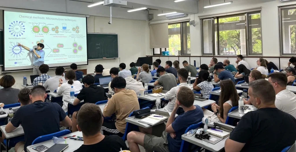
In parallel, SEMI Europe has launched the On Campus programme, designed to connect universities directly with semiconductor companies.
The aim is to expose students to real industry challenges, provide mentorship, and open clear routes into employment. Unlike traditional career fairs, On Campus focuses on sustained collaboration, embedding live industrial projects within academic courses and involving engineers directly in teaching.
The European Chips Skills Academy
The European Chips Skills Academy is another key effort, bringing together universities, training providers, and companies to create a shared skills framework for the semiconductor ecosystem.
It aims to define what “industry readiness” actually means. So, not just technical theory, but practical knowledge of process flows, EDA tools, manufacturing cycles, and quality standards.
Potential international semiconductor campus in Valencia?
I was at a semiconductor conference a few weeks ago where the organiser told me about the plans for an international semiconductor campus in Valencia.
He explained that one of the main priorities for the local government is to support its development.
Mayte Bacete, president of the Valencia Silicon Cluster, also spoke about the project.
She described it as a technological hub designed to train the next generation of professionals, support existing companies, and encourage new ones to emerge.
The goal is to create a place that combines academic excellence, applied research, and real collaboration between universities and industry.
What still needs to change
These initiatives are encouraging, but to make a real difference they need to grow much faster.
From my own experience I can confirm that the demand for semiconductor talent is rising more quickly than these programmes can currently supply.
Here are a few ideas that could help accelerate progress:
Short, intensive bridge programmes
Between graduation and full employment, there’s an opportunity for short, highly practical courses lasting three to six months. These could focus on industrial tools, debugging, verification, process integration, and yield optimisation.
They wouldn’t replace academic degrees but complement them I believe.
Speeding up the transition from theory to productive work.
Embedded industrial internships
Instead of brief placements that only scratch the surface, students should spend at least six months inside companies, ideally linked to their thesis. That’s when learning really sticks.
Shared virtual labs
Access to industrial-grade EDA tools could be expanded through cloud-based platforms. This would allow students from smaller universities to gain exposure to the same design environments used in top semicon companies, levelling the playing field across Europe.
Co-created curricula
Instead of universities updating their courses in isolation, industry should co-design modules on manufacturability, packaging, verification, and supply chain. Many of these areas are missing from current academic programmes but are essential for industry readiness.
Sustainable funding
Pilot lines like NanoIC need long-term financial commitment. Short-term grants are useful for starting projects, but without ongoing funding, these efforts risk fading once the spotlight moves elsewhere.
The bigger picture
This readiness gap isn’t unique to semiconductors though.
Similar patterns seem to appear in AI, robotics, and quantum computing.
Fields where research moves faster than real-world use.
But semiconductors are different in one key way: they’re the foundation for all other technologies.
If Europe can’t close this gap, its entire strategy for technological sovereignty is at risk.
That’s why solving this problem matters!
It’s not just about “better” education.
For me it’s about competitiveness and Europe’s chance to build its own technological future.
A future built on shared tools and shared goals
Europe already has the talent and the research depth. What’s missing is the translation between “labs and fabs”, between professors and process engineers, between curiosity and production.
Initiatives like NanoIC, SEMI On Campus, and the Chips Skills Academy are encouraging signs that this translation is beginning to happen. But for real impact, these bridges need to become scalable.
The goal is simple:
Reduce the time it takes for a graduate to become a productive engineer, and make sure the next generation doesn’t just study semiconductors. They help build them.