
Recruiting Physical Design Engineers: Key Insights
Recruiting Physical Design Engineers is about finding the experts who turn chip designs into physical layouts.
When it comes to semiconductor design, the Physical Design Engineer is the specialist who transforms conceptual ideas into physical layouts. Bridging the gap between design and manufacturing.
Their role is critical in creating high-performance, efficient, and reliable integrated circuits (ICs).
Having recruited for Physical Design Engineers myself, I know how challenging and rewarding it can be to find the right talent for this position. Whether you’re hiring or just curious about this essential role, here’s what you need to know.
What Does a Physical Design Engineer Do?
At a high level, Physical Design Engineers take the logical design of a chip, typically created by RTL (Register Transfer Level) designers, and turn it into a physical blueprint that can be fabricated.
This process involves intricate steps to optimise power, performance, and area (commonly referred to as PPA). Their work ensures that chips meet strict timing, power, and manufacturability requirements.
Key responsibilities include:
Floorplanning and Partitioning
Physical Design Engineers begin by dividing the chip into manageable sections, determining how each module will be placed within the chip’s architecture. When recruiting Physical Design Engineers, I often prioritise candidates who can balance creativity with precision during this critical phase.
Placement and Routing
They determine the optimal placement of components and establish wiring connections between them while minimising delays and ensuring electrical integrity. Experience with cutting-edge placement tools is a major factor when recruiting Physical Design Engineers for high-tech projects.
Timing Analysis and Optimisation
Ensuring the design meets timing constraints is one of the most critical tasks, requiring expertise in static timing analysis tools. From my experience, engineers with advanced timing analysis skills stand out, especially for companies working on tight performance margins.
Power and Signal Integrity Analysis
Engineers analyse power distribution and signal paths to minimise issues like noise, crosstalk, and power leakage. I’ve found that highlighting a candidate’s success in this area is key when presenting them to clients.
Physical Verification
They perform checks such as Design Rule Checking (DRC) and Layout Versus Schematic (LVS) to ensure the design adheres to manufacturing constraints and matches the original schematic.
Physical Design Engineers are multi-skilled problem solvers who ensure that every chip design can become a reality. They juggle technical and practical challenges, making their expertise indispensable in the semiconductor process.
The Semiconductor Ecosystem Explained (in simple terms)
Key Skills and Tools
To excel in this role, Physical Design Engineers need a blend of technical expertise and problem-solving skills. Here are some of the most in-demand tools and competencies:
EDA Tools: Proficiency with industry-standard tools such as Cadence Innovus, Synopsys ICC2, and Mentor Graphics Calibre is essential for tasks like floorplanning, routing, and verification.
Mastery of these tools is one of the first things I look for when recruiting Physical Design Engineers.
Scripting Skills: Languages like Tcl, Perl, and Python are crucial for automating repetitive tasks and enhancing efficiency.
Deep Understanding of Semiconductor Physics: Knowing how signals behave at the physical level helps in debugging and optimizing designs.
Problem-Solving and Collaboration: Engineers must work closely with cross-functional teams, including circuit designers and verification engineers, to resolve conflicts and achieve optimal designs.
Engineers with these skills bring a lot to the table, helping companies optimise chip performance and meet ambitious project timelines. Identifying these strengths early is critical when recruiting.
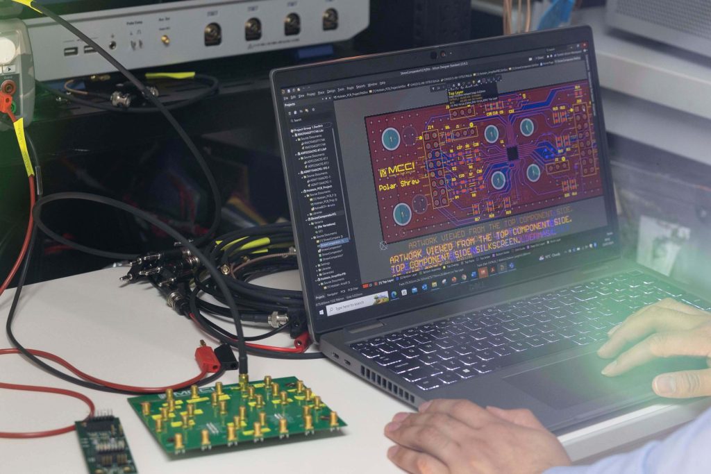
Physical Design Engineers need a blend of technical expertise and problem-solving skills, as they play a key role in ensuring designs can be manufactured efficiently and perform reliably.
Challenges in Recruiting Physical Design Engineers
Hiring for this position isn’t easy. There are many challenges we find when recruiting for semiconductor companies.
When it comes to physical design engineers, the combination of high demand and a limited talent pool creates unique challenges for hiring managers and recruiters alike.
Here are a few common challenges I’ve faced while recruiting Physical Design Engineers:
Talent Shortage
The semiconductor industry is booming, but there aren’t enough skilled Physical Design Engineers to meet the demand. This shortage is one of the biggest hurdles in recruiting Physical Design Engineers, especially for companies outside major tech hubs.High Expectations
Companies often seek candidates with several years of experience and proficiency in cutting-edge technologies, narrowing the talent pool even further. One strategy I use is to focus on transferable skills rather than looking for an exact match for every requirement.
Geographical Constraints
Many top engineers are concentrated in hubs like Silicon Valley or Taiwan, making it difficult for companies in other regions to attract them.
Competition from Big Tech
Large semiconductor companies and tech giants often offer lucrative packages, making it hard for smaller companies to compete.
While these challenges may seem daunting, understanding the market and adjusting your recruitment strategy can make a significant difference. A tailored approach often yields the best results.
To see how each stage of the semiconductor design process connects to specific hiring needs, check out our article on Understanding the Chip Design Flow for Hiring.
Tips for Recruiting Physical Design Engineers
If you’re struggling to find the right Physical Design Engineer, don’t worry. You’re not alone.
These practical tips can help you refine your approach and attract top talent.
To successfully recruit for this role, consider the following strategies:
Target Specialised Communities
Engage with forums like Edaboard, Linkedin groups like this one, and events focused on semiconductor design to find candidates actively working in this niche. In my experience, building relationships in these communities is a cornerstone of recruiting Physical Design Engineers effectively.
Offer Clear Growth Opportunities
Highlight the potential for career progression and access to cutting-edge projects. Engineers in this field often seek roles where they can stay on the leading edge of technology.
Flexibility and Remote Work
While physical design tasks often require access to specialised tools, offering hybrid or flexible arrangements can make your role more appealing.
Collaborate with Expert Recruiters
Partnering with recruiters who specialise in the semiconductor industry can help you find candidates with the exact expertise you need. Having worked in this space for years, I know that recruiting Physical Design Engineers often requires a nuanced understanding of both technical skills and industry trends.
With the right strategies, you can overcome recruitment challenges and secure the skilled professionals your projects need. A proactive approach always makes the process smoother.
Career Path and Outlook
The role of a Physical Design Engineer isn’t just critical today.
It’s a career path with incredible potential for the future. Here’s what you need to know.
Degree
Physical Design Engineers typically hold a bachelor’s or master’s degree in electrical engineering, computer engineering, or a related field. Entry-level engineers start by supporting senior team members on tasks like placement and routing, gradually taking on more complex responsibilities as they gain experience.
Expected Demand
The demand for these professionals is only expected to grow as the semiconductor industry evolves to support technologies like AI, 5G, and IoT. If you’re recruiting Physical Design Engineers, focusing on candidates experienced in advanced nodes (e.g., 3nm or 5nm technology) will set your company apart.
As technology advances, the demand for Physical Design Engineers will only increase.
Investing time and resources into recruiting and nurturing talent now can future-proof your team.

Why Physical Design Engineers Matter
Every chip that powers our devices owes its existence to the work of a Physical Design Engineer. Their role is pivotal in ensuring that technology keeps evolving.
Without Physical Design Engineers, the transition from logical design to a manufacturable chip would be impossible. Their work directly impacts the performance, power efficiency, and size of the final product, making them indispensable in the semiconductor development process.
Conclusion:
Having worked extensively in recruiting Physical Design Engineers, I’ve seen firsthand how critical these roles are to the success of semiconductor projects. By understanding their value and hiring the right talent, companies can stay competitive in this ever-evolving field.
Up to Your Next Physical Design Hire
In semiconductor hiring, recruiting Physical Design Engineers demands a thoughtful approach that takes into account the unique challenges and opportunities within this specialised field.
From floorplanning and routing to timing analysis and physical verification, Physical Design Engineers bring a diverse set of skills that are essential to turning conceptual chip designs into manufacturable realities.
Understanding the nuances of their roles, along with the market dynamics and motivators that attract top talent, can help you navigate the recruitment process with confidence.
Whether you’re overcoming talent shortages or seeking niche expertise, I hope these insights provide a strong foundation for your next physical design hire.
For more insights or connections in semiconductor recruitment, feel free to connect with me on LinkedIn HERE
Need Help Hiring Physical Design Engineers?
Contact me here

Claude Loeffen
Semiconductor Headhunter