Understanding the Chip Design Flow for Hiring and Workforce Planning
Introduction
Over time, through many conversations with semiconductor engineers, design experts, and hiring managers, I’ve come to appreciate just how complex the world of chip design really is.
The process of turning an abstract idea into a functioning microchip involves not only technical excellence but also incredible teamwork, planning, and coordination.
From a workforce and hiring perspective, I’ve found it essential to develop a good understanding of the chip design flow. Because for me it’s the foundation for recognising the specific skills, mindsets, and collaborations required to bring a chip to life.
I’m not a technical expert myself, so my goal here is to explain the chip design process in a straightforward, easy-to-understand way.
Focusing on how it works in practice and why it matters from a human and organisational perspective.
Specification
Where It All Begins
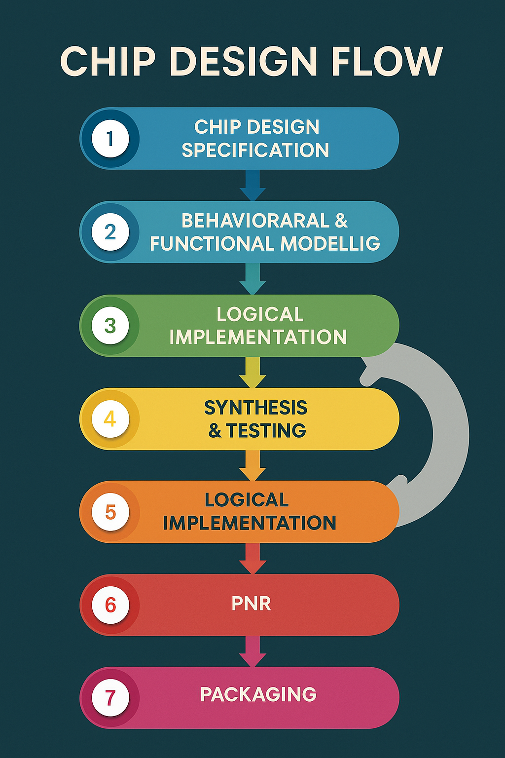
Every chip starts with an idea, a need, a function, or a specific performance target. This early phase is all about specifications, which means defining what the chip must do, what constraints it must meet, and what technologies it will use.
I’ve learned that this stage often involves system architects and project leads who balance technical vision with practical limitations like budget, time, and manufacturability.
People who can connect technical ideas with overall planning usually do well at this stage.
Design Entry
Turning Ideas into Schematics
Once requirements are clear, the next phase involves translating them into actual circuit designs.
Digital designers write code in hardware description languages such as Verilog or VHDL, while analog designers draw circuit schematics using specialized software like Cadence Virtuoso.
From what I’ve learned, digital design is much more automated, while analog design is still a very manual and creative process. Analog engineers often describe it as “engineering meets artistry.”
For hiring purposes, these differences matter.
Digital design tends to value coding and automation, whereas analog design rewards intuition and experience.
Each part of the design flow needs engineers with specific skills and experience. Finding people who really understand these areas isn’t always easy, especially in roles like IC Design.
RTL Design
When it comes to hiring for digital design teams, RTL engineers are often at the core of the process. They translate abstract specifications into the logic that makes a chip function. It’s where ideas start to take real, testable shape.
Through my experience in semiconductor recruitment, I’ve learned that finding strong RTL talent requires more than just assessing technical skills.
The best candidates combine problem-solving ability, attention to detail, and a clear understanding of how their work connects to the broader design and verification flow. Building teams with this kind of talent early on sets the foundation for a smoother project and better overall design outcomes.

Simulation and Verification
Testing on Screen Before Reality
Before anything is physically built, designs go through simulation and verification. Engineers use complex software to model how electrical signals behave, testing for things like gain, power usage, or timing accuracy.
In practice, this stage is where verification engineers truly make a difference.
Professionals who excel at problem-solving, attention to detail, and persistence.
Many of them describe their work as “finding the needle in the haystack,” ensuring that every possible design scenario has been checked.
From a workforce standpoint, these roles are crucial.
They reduce costly mistakes later in production and are often the backbone of quality assurance in any semiconductor team.
From a hiring perspective, finding strong verification engineers can be challenging, as the role requires a mix of analytical thinking, patience, and deep tool knowledge. But, investing in these profiles early can save a company significant time and resources down the line.
Layout Design
The Blueprint of the Chip
After the logic and functionality are validated, the design moves into layout, effectively creating a physical blueprint of the chip. Using design software, layout engineers decide where each transistor and wire will go, following strict spacing and size rules set by the chip manufacturer.
One designer once told me, “Layout is where engineering meets geometry.” It requires precision, patience, and an eye for detail. Layout engineers are rare and highly sought after, particularly those familiar with multiple technology nodes. From a hiring perspective, this specialisation often defines the bottleneck in scaling design teams.
The physical design phase is where the chip layout really takes shape and the performance targets need to be hit in real silicon. If you’re curious about what companies are looking for when recruiting Physical Design Engineers, you can check out this article here.
Parasitic Extraction and Post-Layout Simulation
Even after the layout is drawn, the work isn’t done. The physical connections add small, unintended electrical effects. Tiny resistances and capacitances called parasitics.
Engineers must extract these and run another round of simulations to make sure the chip still works as expected.
This step blends physics, software, and intuition.
It’s also a great example of where collaboration is key.
Designers, layout specialists, and manufacturing liaisons must all speak the same language. In workforce terms, this is where cross-functional communication really proves its value.
Design Rule Checks and Final Verification
Before manufacturing, the design undergoes more rigorous checks. Design Rule Checks (DRC) to ensure it can actually be fabricated, and Layout vs. Schematic (LVS) to confirm that the physical layout matches the intended circuit.
I see the engineers that work in this area as the gatekeepers of quality.
Their experience prevents expensive manufacturing errors.
When hiring for these roles, I’ve learned to look for engineers with a very detailed mindset. Basically people who take pride in details and follow structured processes.
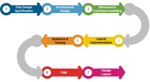
Tape-Out
The Big Send-Off
“Tape-out” is the term engineers use when the final design is ready to be sent to the foundry for fabrication. It’s a moment of both relief and nervousness, after months of simulation and checks, the chip is finally on its way to becoming real silicon.
The costs here are significant, sometimes tens of thousands of dollars per square millimeter in advanced technologies. From a leadership point of view, this step highlights the importance of accountability, documentation, and experience. Teams that have been through several successful tape-outs are incredibly valuable assets.
It’s also important to think about how people learn the skills needed for each step in the design flow. Many engineers start building these skills during their studies, long before joining a company.
If you want to read more about how education and industry can work better together in semiconductors, you can find that here
Packaging
Giving the Chip Its Physical Form
Once manufactured, the chip still needs to be packaged, enclosed in a protective housing that allows it to be connected to other components. Depending on the application, packaging can be as simple as a small plastic case or as advanced as multi-layered, heat-control structures.
Packaging engineers often come from materials science or mechanical engineering backgrounds. It’s a reminder that chip design isn’t just electrical, it’s a truly interdisciplinary field involving physics, materials, and design for manufacturability.
Testing and Validation
Making Sure It Works
After packaging, the chip goes through testing to confirm it behaves as expected under various conditions. Engineers measure things like performance, power efficiency, and temperature tolerance.
I’ve found that test engineers often blend hardware knowledge with programming skills to automate test setups. These hybrid profiles are becoming more valuable as companies move toward faster prototyping and AI-assisted validation.
Iteration and Improvement
Even after months of work, the first batch of chips rarely comes out perfect. Small adjustments are often needed, maybe a timing tweak or a layout refinement. This iterative loop is part of what makes semiconductor design such a continuous learning process.
From a hiring perspective, this is where adaptability and collaboration are really important. Teams that learn from test results and communicate effectively tend to improve with every revision.
In fact, what you will find is that many companies intentionally hire engineers with a growth mindset, people who see each iteration as a chance to get better.

The Human Side of Chip Design
What I’ve come to appreciate most after learning about all these stages is how human the process really is. I see it as a web of interconnected expertise: analog designers, digital specialists, layout experts, test engineers, and project managers. All contributing their piece of the puzzle.
Each phase requires a different mindset, and as someone who looks at this from a talent and workforce planning point of view, I’ve seen how essential it is to have not just skilled individuals, but well-balanced teams.
“Chip design isn’t just about knowledge, it’s about collaboration, patience, and shared problem-solving” a design manager once told me.
Each stage of chip design relies on specialised expertise. something that effective semiconductor recruitment practices can make or break.
Learn how our semiconductor recruitment expertise helps companies build world-class design teams.
My Final Thoughts
The chip design flow, from concept to silicon, is both technical and human.
It’s about creativity guided by precision, and teamwork driven by shared purpose.
Over time, I’ve learned that successful chip projects depend as much on team structure and talent alignment as they do on advanced tools or processes.
In a world where technology evolves at lightning speed (literally in photonics), it’s the blend of people, knowledge, and collaboration that turns an idea into a functioning piece of silicon, and that, to me, is what makes chip design so fascinating